Copper plating is widely used across industries such as PCB manufacturing, semiconductor packaging, electroforming, electronics, electrochemical equipment, and corrosion protection systems. Among the available technologies, electroless copper plating and electrolytic copper plating are the two most commonly used processes.
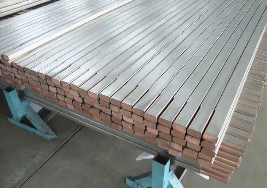
Although both methods deposit a copper layer onto a substrate, they differ significantly in deposition mechanism, coating uniformity, conductivity, thickness control, and production cost. Stable, corrosion resistant conductive components are indispensable to support the stable operation of both plating processes. Our core product, titanium clad copper composite materials, has become the preferred conductive hardware for most copper plating workshops and electrolysis plants. Understanding these process differences and matched conductive materials helps manufacturers select the most suitable plating process and supporting busbar/rod products for their applications.
What Is Electroless Copper Plating?
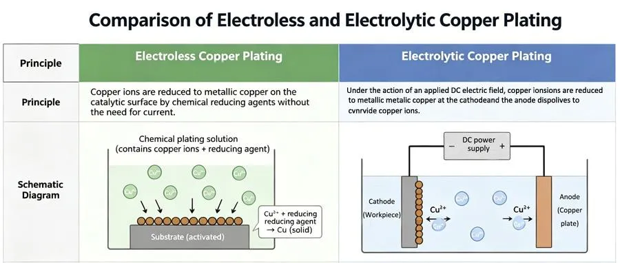
Electroless copper plating, also known as autocatalytic copper plating, deposits copper onto a substrate through a chemical reduction reaction without the use of external electrical current. The process typically involves:
Surface cleaning and activation
Chemical reduction of copper ions
Continuous coating growth through autocatalytic reaction
Advantages of Electroless Copper Plating
Excellent coating uniformity
Suitable for complex geometries and deep holes
Can plate non-conductive materials
Ideal for PCB through-hole metallization
Limitations
Slower deposition rate
Higher chemical consumption
Higher operating costs
For PCB factories adopting electroless copper plating lines, our lightweight titanium clad copper racks and conductive frames effectively avoid copper ion contamination from pure copper hangers. The titanium outer layer resists corrosion from chemical plating solution, ensuring stable plating quality for circuit boards while cutting rack replacement costs.
What Is Electrolytic Copper Plating?
Electrolytic copper plating uses electrical current to deposit copper from an electrolyte solution onto a conductive substrate. The process involves:
Conductive workpiece acting as cathode
When current passes through the electrolyte, copper ions migrate and deposit onto the surface.
Advantages of Electrolytic Copper Plating
Suitable for large-scale production
Limitations
Less effective for blind holes and deep cavities
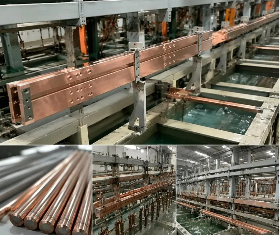
Mass electrolytic copper plating production lines demand high-current conductive components. Titanium clad copper busbars, beams and round rods perfectly combine copper’s ultra-high conductivity and titanium’s acid & alkali corrosion resistance. They deliver even current distribution, reduce voltage drop, and greatly extend service life compared with traditional solid copper conductors.
Industrial Applications
Printed Circuit Boards (PCB)
Electroless copper plating is commonly used to create conductive layers inside drilled holes before electrolytic copper plating increases thickness. Titanium clad copper conductive fixtures support both pre-plating chemical tanks and follow-up electrolytic copper plating stations for consistent PCB mass production.
Semiconductor Packaging
High-precision electronic components require uniform copper coatings that can only be achieved through electroless deposition. Mini customized titanium clad copper conductive rods are widely applied in precision semiconductor electroplating equipment to eliminate impurity pollution.
Electroforming and Precision Components
Electrolytic copper plating provides rapid thickness build-up and excellent conductivity for industrial components. Large current titanium clad copper busbars serve as main conductive parts for electroforming equipment.
Electrochemical Equipment
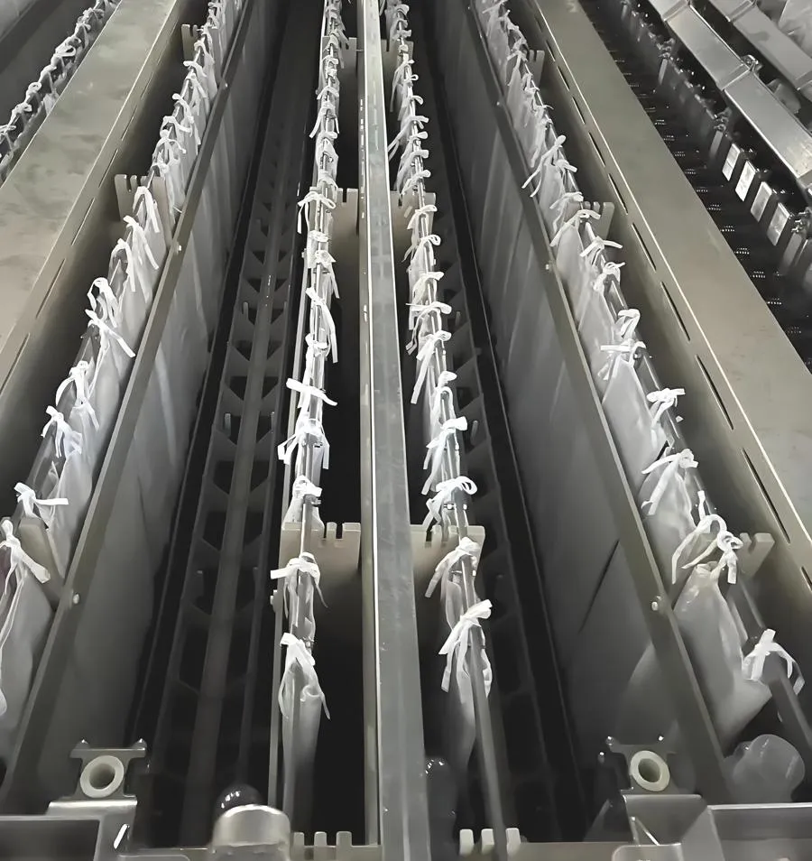
High-performance conductive parts are the core foundation of stable copper plating. Titanium clad copper busbars and composite rods balance excellent electrical conductivity of copper and full anti-corrosion protection from titanium outer layer. They are the standard conductive hardware adopted in mass copper plating workshops, electro-winning plants, electro-refining facilities, chlor-alkali production and all kinds of surface treatment lines, solving the problems of copper corrosion, uneven current and frequent maintenance of traditional pure copper conductors.
Selecting the Right Copper Plating Process & Supporting Conductive Materials
The choice of plating technology depends on product geometry, conductivity requirements, coating thickness, production volume, and overall cost considerations.
Electroless copper plating is preferred when coating uniformity and complex geometries are critical. It matches small & medium-size titanium clad copper plating racks for chemical plating tanks.
Electrolytic copper plating remains the preferred solution for high-volume production requiring thick, highly conductive copper deposits. Large-size titanium clad copper busbars and anode beams are the standard matching conductive components for such production lines.
As industries continue demanding higher efficiency, longer service life, and improved electrical performance, both copper plating technologies will remain essential manufacturing processes across electronics, energy, and electrochemical sectors.
No matter your workshop runs electroless copper or large-batch electrolytic copper plating, our factory supplies customized titanium clad copper busbars, round rods, hanger beams and conductive fixtures of all specifications. Our composite material perfectly adapts to various plating electrolyte environments, lowering your long-term operation and maintenance costs. If you need technical data, sample testing or custom drawing design for electrochemical conductive parts, feel free to contact our engineering team for one-stop solutions.


 +86-731-82224155
 8613272400394
 enquiry@jetvisiontitanium.com